
In July I posted: don't ask an AI to make you a STEP file — ask it to write the program that makes the STEP file.
It started as a tip at the end of the PCB symbols and 3D models article, and it's still the most-read thing I've put out this year.
I practice what I preach — here's me using that advice to make a real part, and it worked on the first try.
A while back I started building a generic firmware test rig. It's a fleet of microcontroller dev boards hanging off a custom USB carrier PCB for agents to use. This has been taking up a ton of space on my bench as a pile of boards and cables.
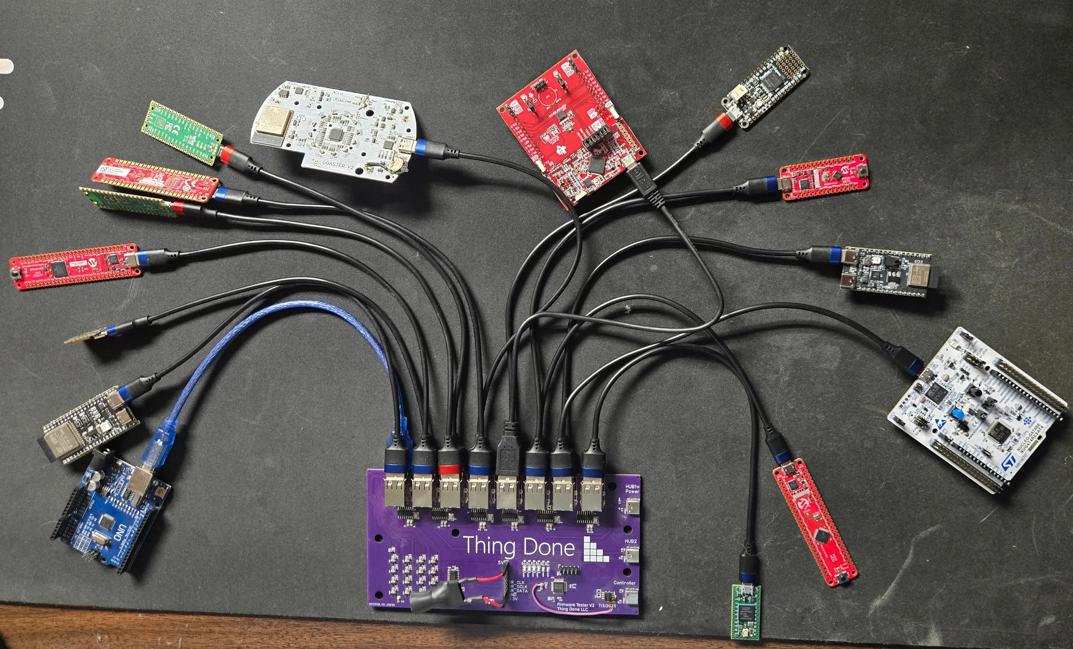
So I took my own advice, start to finish. The enclosure printed right the first time, and the PCB dropped straight in.
What the AI got from me
Not much. A crude sketch, and the fabrication outputs I already had for the carrier board: the Gerber ZIP, a DXF, and the OBJ/MTL 3D export from the layout tool.
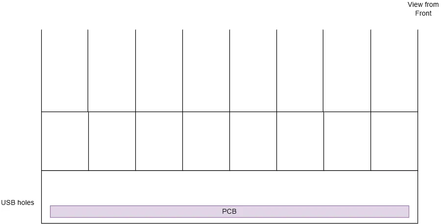
That's the whole spec. I never measured the board by hand, and I never opened a CAD tool to model anything.
I kicked it off and walked away
Here's the part I want to be honest about, because it's the part people don't believe: my total hands-on time was just under an hour, squeezed in between other things on a Friday afternoon.
I went back through the timestamps to check myself. 2:38 PM: made the repo. 2:47: dropped in the fab outputs from the board. 3:05: saved the sketch. Then I spent a few minutes with a planning agent turning the sketch into a task list — four phases, 33 tasks, every design decision made up front (3 mm walls, 2 mm board clearance, open front and back, print face-down, don't stop to ask me anything). After that planning agent wrote up the tasks, I did a cursory review. At 3:34 PM, I kicked off the run and went on with my day.
The agent worked through the list on its own: measure the Gerbers, build the model, write the tests, generate the print files, committing and pushing as it went. Individual tasks ran anywhere from 4 to 41 minutes. At 11:14 PM it hit a wall — the model provider was at capacity — and the run stalled. It resumed and pushed the final verified release at 2:12 AM. 33 tasks in 10 hours 42 minutes of machine time vs <1 hour of my time.
My involvement between kickoff and done was essentially zero (I'm unsure if I hit resume or if it resumed on its own).
I woke up to a repo with the STEP, the STLs, the dimensioned evidence views, and a passing test suite. Then I hit print.
What the AI built
Here's the part that matters: the deliverable was never a STEP file. It was a Python program — build123d for the solid modeling, gerbonara for reading the Gerbers — that derives the enclosure from the board's own fabrication data.
The program measures the board outline straight from the Gerber (175 × 90 mm). It cross-checks the DXF and the 3D OBJ against that outline — fitting the transform between coordinate frames and refusing to continue if the sources disagree. It finds the three USB connectors on its own, by clustering the OBJ mesh and correlating the candidates with the copper and silkscreen in the Gerbers. All of that gets written into a calibration record bound to the SHA-256 of every input file, so if I rev the board, the build refuses to run against stale measurements.
Then it generates the housing: a monolithic 185 × 100 × 154 mm print with 3 mm walls, divider fins forming the bays for the dev boards, the carrier PCB in the base, and the three USB apertures cut through the side wall exactly where the connectors are.
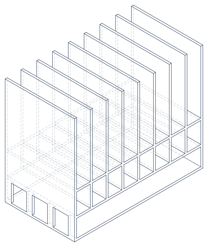
The program argues for its own printability
This is where writing a program beats generating an artifact by a distance. Because the geometry is code, the AI could write checks against it — and it checked it, without much prompting beyond "I want to print this without supports."
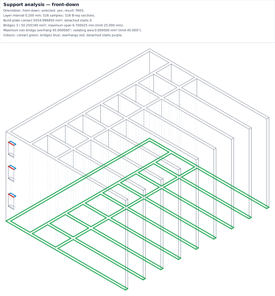
The build slices the model at every 0.2 mm print layer — 526 actual B-rep sections per candidate orientation — and enforces the FDM rules: nothing detached mid-air, no overhang steeper than 45°, no unsupported bridge longer than 25 mm. It evaluates both viable orientations, scores them, and picks one deterministically. The result ships as an evidence image, not a promise:
The fit side gets the same treatment. Every USB aperture is checked against the measured connector envelope with 2 mm of allowance, insertion lead-in chamfers on the outside edges — and it deliberately skips the chamfer on the floor-adjacent edges, because cutting there would thin the 3 mm floor member it needs for the print. That's the kind of decision I'd expect from a careful junior engineer, and it's sitting in a dimensioned section view I can audit in ten seconds:
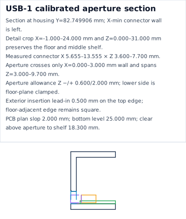
In total the project ended up as a small CAD pipeline: about 16k lines of Python with 105 tests, producing the STEP, the print STLs, nine dimensioned SVG evidence views, and a manifest with checksums for everything.
The print
The print took 47 hours and 24 minutes on my old Elegoo Neptune 2 Pro (it's a ~$200 3D printer from ~2022). I printed it in PLA, ran out of filament two-thirds of the way through and swapped in a new spool, and it finished without incident.
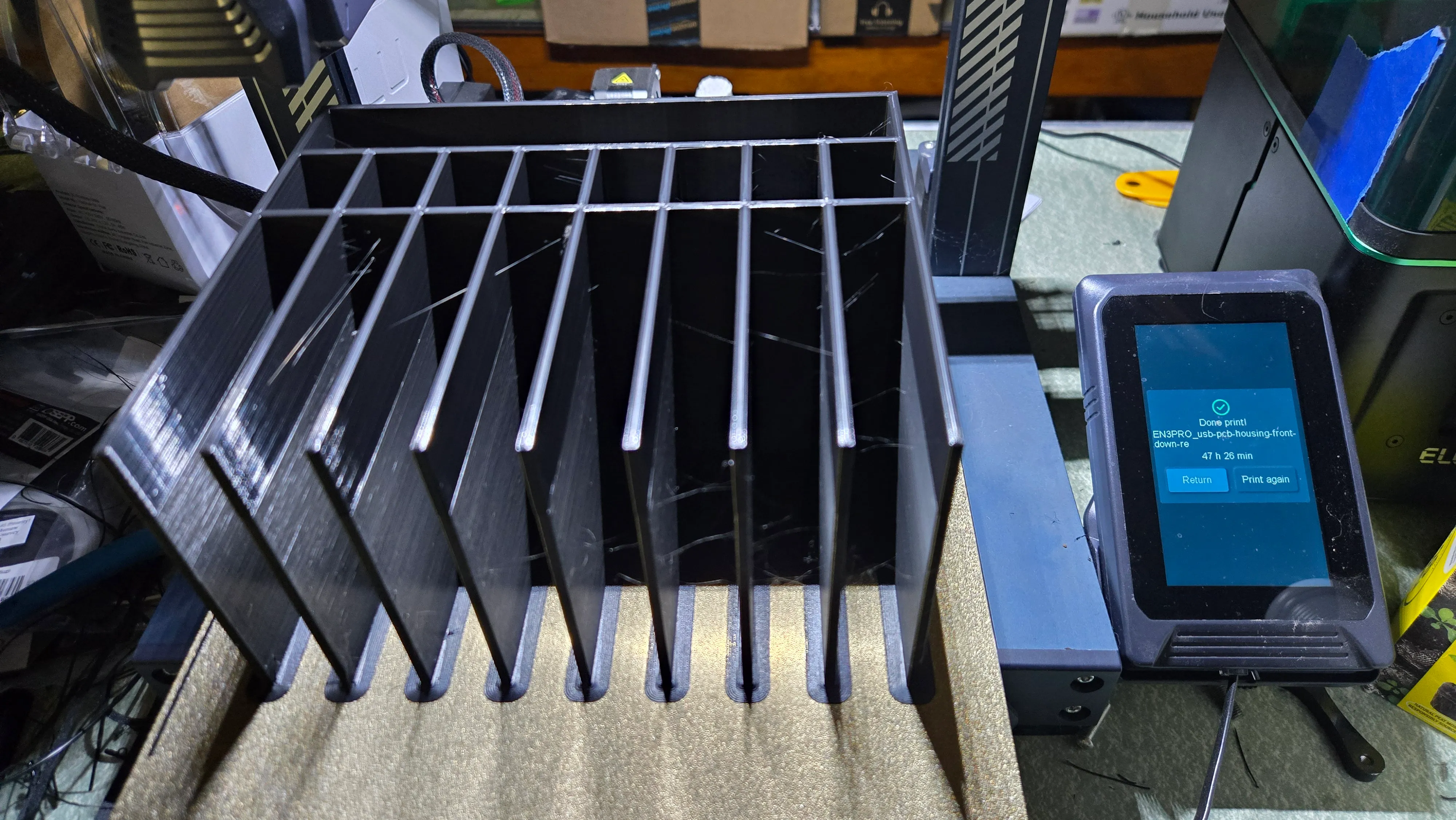
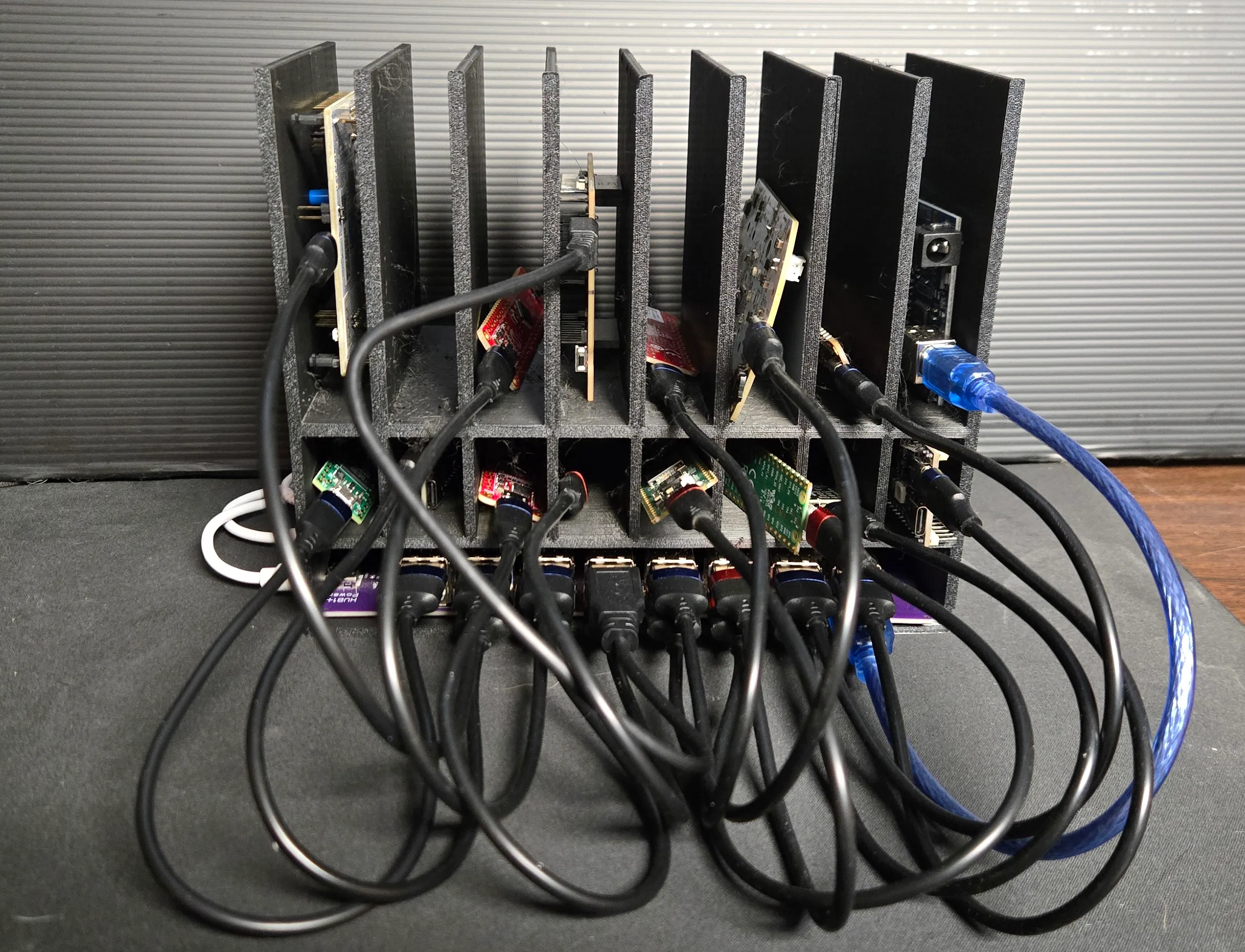
The print is solid, the walls are thick, and the USB connectors line up perfectly with their apertures.
It worked on the first try. No wasting a ton of time on a printer iterating; no rev B of the enclosure. It just worked.
Why the program wins
If I'd asked an AI for a STEP file directly, I'd have gotten something that looks like an enclosure. It might have worked, but it could have failed (even with a top tier model). Best case it would have wasted a ton of time figuring out a way to test and iterate on it.
Current models can't reliably emit valid solid geometry — but they are genuinely good at writing and debugging code against tests.
Don't assume your AI can one-shot everything. Instead ask for something it can iterate on. And leveraging their strengths (writing code and tests) is more reliable.
These models are really built to build software. So we leverage this by turning our physical problem into a software problem.
- It re-runs. If I want anything changed or tweaked, it can make those changes parametrically and re-run the build, producing a new STEP and new evidence views. I can even change the board revision and have it measure the new Gerbers and re-derive the enclosure.
- It refuses to be wrong quietly. It wrote unit tests for its own measurements, collision-checks the assembly, and verified nothing was silently off by a millimeter — the kind of error that fails a print.
- It shows its work. The dimensioned evidence views meant I can do a quick review of the design from images, the same way I'd review a drawing — without opening a CAD tool once.
- It knows why it's printable. I said "no supports" — so it enforced the 45° rule and the bridge limits in code.
The STEP file is disposable. The program is the asset.
What the rig is for
This enclosure is one piece of a bigger project: an agent-safe rig for running firmware experiments across a fleet of microcontroller dev boards — different vendors, different architectures, all measured the same way. I've been having agents working on firmware on several projects — this is a harness for them to test/debug without each of them needing physical access.
I've also been comparing and benchmarking different microcontroller boards in the process.
That's a series of articles on its own that I'll start uploading shortly.
If you're trying to figure out where AI fits your hardware process, I'm happy to talk.